Home Hardware, Part 2: Width Matters
We’re back! Not with rework. This time we’re talking about impedance and review. Apparently I can get into a heated argument about a board before it even gets here.
In part one, I wrote about using Codex to design my own hardware because I’m sick of Control4, Savant, and the rest of that shit. The useful part wasn’t one-shotting a PCB. It was having the agent work through datasheets, compare parts, and check the design. Then I had to notice that the connectors were facing the wrong fucking way.
There was more to review.
Which board are we arguing about?
I was talking through the Sensor Hub’s RF layout with Paul, and we were getting different answers for the impedance. This turned into a pretty heated argument, which might have scared some of the other people in the room. Honestly, we were just trying to figure it out.
Paul started with this impedance calculator. I kept annoying him because I still didn’t understand why we were getting different numbers. Eventually he switched to JLC’s calculator, which was what the model was using. I wanted to understand the model’s math and compare it with his.
The KiCad view was part of the confusion. The connection looked orange,
and the second interior layer, In2.Cu, was orange in the layer list.
The first interior layer, In1.Cu, was green. So we thought ground was
on the second one, and kept arguing about the thickness between layers.
Then I realized both interior layers had ground copper, with ground vias connecting across layers. Seeing orange didn’t mean the connection was only on that layer. There was ground on the green layer too, right under the RF trace. The model was right! I was just trying to understand what it was telling me.
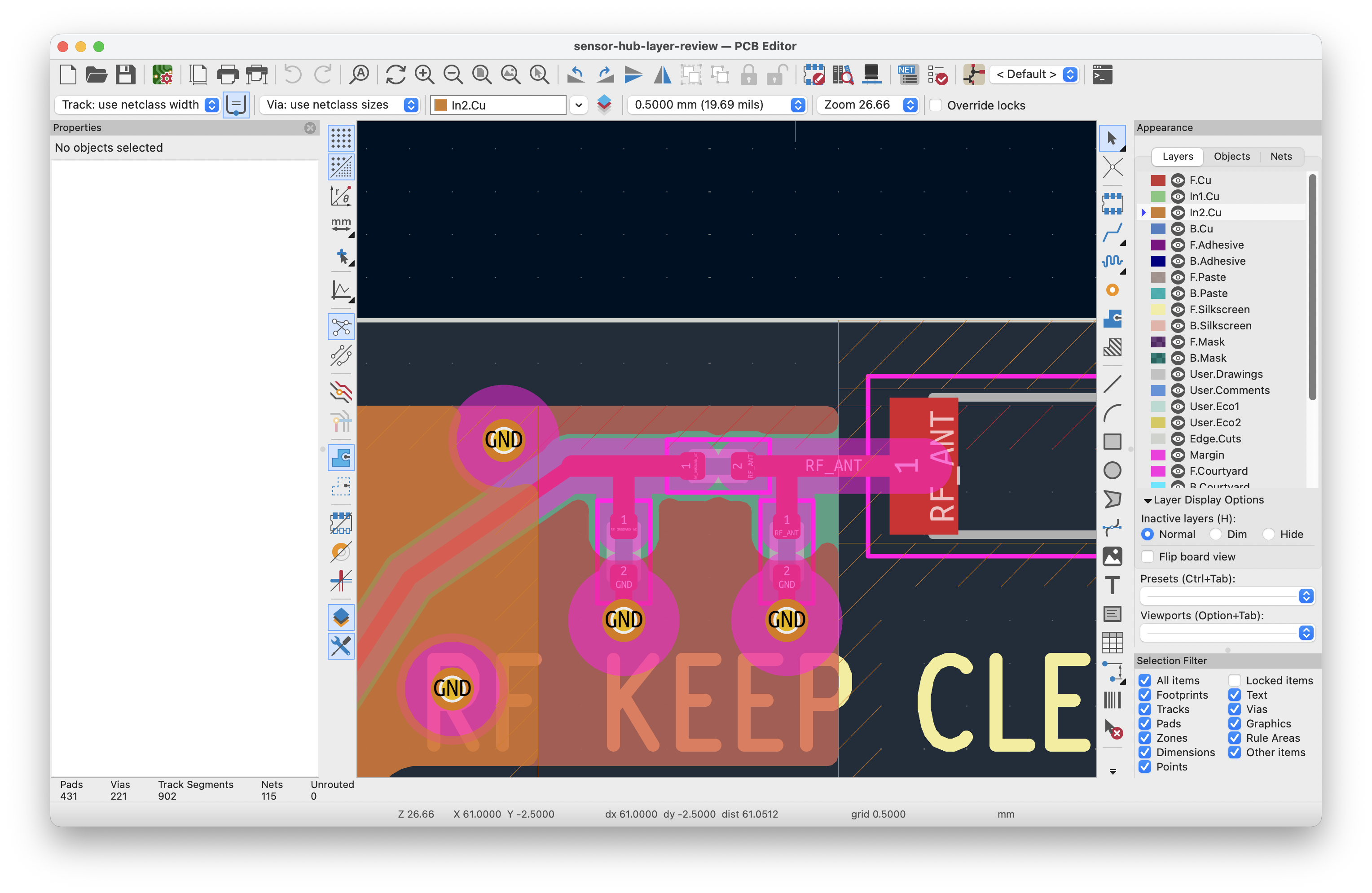
The confusing view, recreated in KiCad. In2.Cu is selected in orange;
the green In1.Cu ground is there too.
The RF trace is on F.Cu, the top layer. There is 0.1164 mm of
insulating material between it and the first inner ground plane. If we
used the second inner layer as the reference, we’d be including the thick
core between the two inner layers as well. The whole board is nominally
1.6 mm thick, but that isn’t the distance from this trace to ground.
For this feed, I want a characteristic impedance of 50 ohms. I had been looking at the trace width, but the calculator also needed the copper thickness, dielectric material, and gap to the ground beside it. That’s why I kept asking about the layers. If Paul and I used different distances to ground, of course we’d get different answers.1
Special, apparently
Then there was the board style in JLC’s calculator. The agent was using JLC04161H-2116, which has “Special” next to it. I wanted to know why it had picked that one in the first place.
It had originally designed around 0.137 mm between the outer layers and their references for the Sensor Hub, and 0.150 mm for Maintenance. Neither was the actual JLC construction it eventually selected. Of the options it compared, 2116’s 0.1164 mm was closest, so it picked that and recalculated the trace widths. That was its reasoning. It wasn’t that my boards needed to be special.
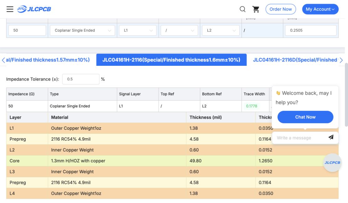
This is the 2116 calculation from the review.
Look at what happens if I change the board style and leave the target, signal layer, reference layer, and side-ground gap alone:2
| JLC stackup | Top copper to inner ground | Width for 50 ohms |
|---|---|---|
| JLC04161H-2116 | 0.1164 mm | 0.1778 mm |
| JLC04161H-3313A | 0.2064 mm | 0.3203 mm |
Almost twice as wide! Paul’s number was roughly 0.34 mm. I don’t have every setting from his calculation to recreate that, but look how much one choice in JLC changes the answer. This is the shit we were arguing about.
I’d been calling them “special” and “normal,” and it turns out JLC labels both of these particular options “Special.” Of course. We needed to use the actual stackup names and make sure we were calculating the same fucking board.
Okay, but what’s in the file?
JLC gave 0.1778 mm, so I asked if that was the width in the PCB file. It was 0.1800 mm. Why show me a width if that’s not the width you’re using?
The agent had an explanation for this too. It had two different answers depending on whether there was ground beside the trace: 0.1778 mm with it, 0.1814 mm without it. So it picked 0.18 mm in between. The decision was documented; I just hadn’t understood that was why the PCB didn’t match the number it was showing me.
I told it to change the width to 0.1778 mm. That’s 2.2 micrometers, or about 1.2%. I know, this is a tiny fucking difference. I still wanted to understand what it meant, which is why I was asking Paul about it.
Then I got to be annoyed at the calculator too. Put in 0.18 mm and ask what impedance that gives: 49.924 ohms. Do the same for 0.1778 mm: 50.221 ohms. I had asked for the more precise width, and now it was farther from 50 ohms in the calculator. Lol.3
The other thing I wanted reviewed was the 0.25 mm width used for some short launches and matching sections. The calculator gave 42–43 ohms when I entered those as uniform lines. Well, they’re short transitions, so there’s more to check there. I still want it to check!
It can read the PCB file and follow the route. Where does the width change? How big is the gap beside it? Which ground is underneath it? Having to ask about each little bit myself is fucking annoying. That’s why I’m using an agent in the first place.
Do I even need four layers?
I’m also switching both boards to two layers. James and Paul both gave me shit for the four-layer boards with two ground planes! I think I made the agent over-rotate on the datasheets. I kept telling it to follow the datasheets, and Espressif recommends four layers for the ESP32-S3. So that’s what it did. But I wanted it to think about whether I actually needed four. Espressif has instructions for two layers too! These aren’t particularly crazy boards, so I want to try that.
I should probably be more specific when I tell it to keep things clear underneath. I mean the antenna keepout. I still need a continuous ground plane for the chip, RF, and crystal. And the less shit routed on the bottom, the better.4
Codex said I might pay about the same for two layers or four on a small order.5 I care more about what happens when I order a bunch of them, so I’ll compare those quotes too. Maybe I don’t get much of a saving now, but I don’t want to keep paying for layers I don’t need. Fucking economies of scale again.
There is a tradeoff: JLC’s controlled-impedance service starts at four layers.6 On two layers, I can work out the width myself, but I haven’t bought the same impedance guarantee. I also have to calculate it again for the new distance to ground. I can’t spend all this time arguing about 0.1778 mm and then copy it onto a different stackup.
It’s not a schematic!
James had a different problem with the design:
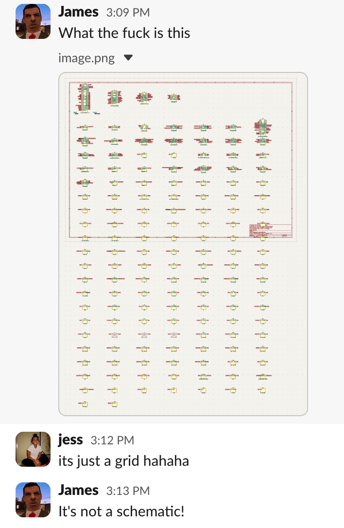
Fair. Super fucking fair.
It was just a grid hahaha. The agent had lined up all the components and connected them with net labels. This was fine for KiCad, but James was right. What the fuck is someone supposed to do with that?
I want to look at a power supply and see the feedback path, or look at a chip and see its decoupling capacitors next to it. I don’t want to go find each of those symbols somewhere else on the page. Neither does anyone I’m asking to review this.
I had Codex redraw it into functional sheets and compare the pin connections before and after, to make sure rearranging it hadn’t changed the circuit. I’m happy to have it do all that shit. But I still have to look at the result, or I get a very thoroughly checked grid.
The part I still have to measure
I asked Paul what being off on the width would actually do. When he explained the possible effects on heat and range, I was like, well, fuck, this is going into a J-box. I’m trying to make the Sensor Hub work at 140°F (60°C) ambient, plus the heat it generates itself. And I started this whole thing because I wanted better Bluetooth range.
Paul helped me understand why I should care about this stuff. I was worried I’d made something that would get hot in the box and have worse range, which would be pretty fucking annoying given what I was trying to build.
But I was giving 2.2 micrometers a lot of responsibility. I still hadn’t measured heat or range. And I was mixing up loss with the signal reflected by a mismatch, which doesn’t all turn into heat in the trace.7
So yes, I’m going to check the antenna matching and RF path. Then I get to try the range and run the boards under load at temperature to find out if I should actually have been worried. Until I’ve verified they work, I’m keeping the repo private. I know, I said hopefully the second post. You’ll have to wait for the hardware too.
Overall, though, I think the boards I ordered should be okay-ish as far as this tiny width discrepancy goes. The long feed was already close to 50 ohms in the calculation. This wasn’t evidence of a bad antenna, or a discovery that the boards were fucked. I still need to test them. Maybe I’ll have some rework for you next time.
The model I used was “Coplanar Single Ended” in JLC’s calculator. It includes ground on either side of the trace and underneath it. These are characteristic-impedance calculations. I’m not expecting to get 50 ohms with a multimeter across a piece of copper.
[return]My inputs on September 9 were four layers, nominal 1.6 mm, 1 oz outer copper, and 0.5 oz inner copper. I entered a side-ground gap of 0.2505 mm; the result displayed 0.2504 mm. You can put those into JLC’s calculator and change the construction yourself. Here’s the stackup table. I haven’t measured the boards.
[return]I couldn’t get exactly 50.000 ohms going back and forth between asking for a width and asking for an impedance. JLC’s copper thickness assumption isn’t quite the same as the nominal copper I have in KiCad, either. I need to keep both of those things in mind before declaring one number better.
[return]Here’s the ESP32-S3 layout guidance. I still need to follow the antenna’s instructions too.
[return]Here’s the deal: five standard 100 × 100 mm boards from $2, with 1–4 layers. That’s what Codex was going off. I checked on September 9. Now they make you use their desktop app for the $2 deal. Of course they do. That’s bare boards, before parts, assembly, shipping, or taxes. I haven’t compared quotes for both versions of my assembled boards yet.
[return]Here’s what JLC offers. That little tolerance field in the calculator doesn’t mean they promised me anything.
[return]More on measuring reflections, for anyone else now wondering where the signal goes.
[return]